Build a LocoIO Inverter
Build an add-on logic inverter daughterboard for an HDL LocoIO
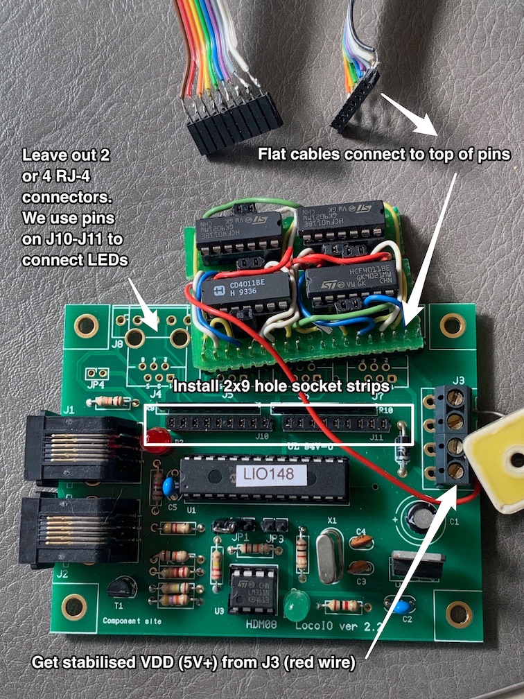
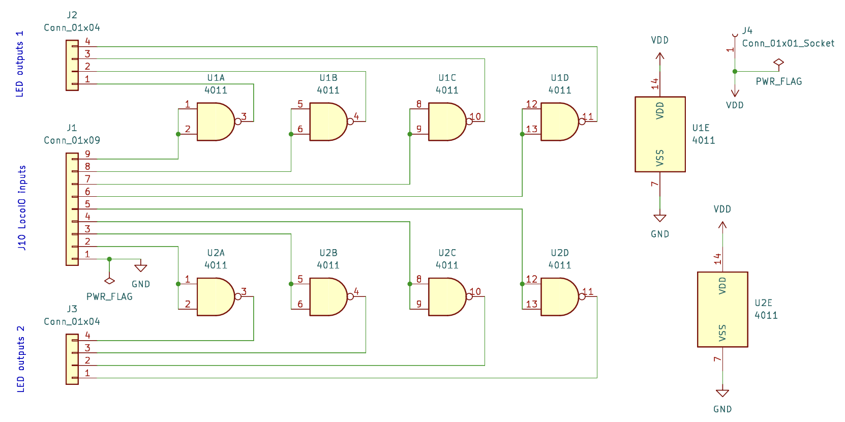
To reduce the number of outputs required to connect a switch panel to Loconet, I designed a small PCB with 4 CMOS 4011 IC’s. Every output pin on J10/J11 is inverted to a second LED on the panel, simply because I don’t have switch feedback and if a switch isn’t thrown, it’s supposed to be closed.


Components (for 8 outputs):
| Item | Qty | Description | |--------|-----|-------------------------------------------------------------------------------------------------------------------------------------------| | J1 | 1 | Connector_PinSocket_2.54mm:PinSocket_1x09_P2.54mm | | J2, J3 | 2 | Connector_PinSocket_2.54mm:PinSocket_1x04_P2.54mm | | J4 | 1 | Connector_PinSocket_2.54mm:PinSocket_1x01_P2.54mm | | U1, U2 | 2 | Quad Nand 2 inputs, x4011 DIP-14 IC ([Datasheet](https://www.intersil.com/content/dam/Intersil/documents/cd40/cd4011bms-12bms-23bms.pdf)) |

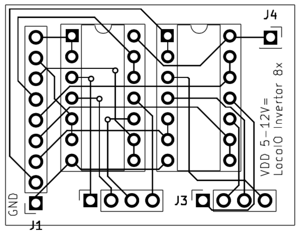
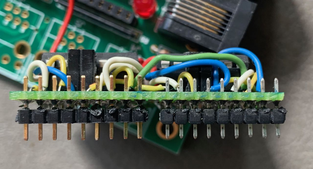
I built mine using a 18x15 hole piece of Euro-PCB experimenting board with pass-through pins for the original outputs, but you could have a PCB made using KiCAD from these KiCAD files.

Enjoy Reading This Article?
Here are some articles you might like to read next: